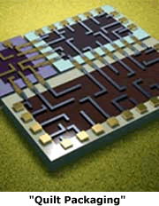
A team of University of Notre Dame researchers led by Gary H. Bernstein, professor of electrical engineering, has demonstrated a new technology for inter-computer chip communication calledQuilt Packagingthat may further the evolution of high-performance electronic systems.
The semiconductor industry has long promoted an international technology roadmap that corresponds withMoores Law in stating that the density of chips doubles approximately every 18 months. Due to the laws of physics, the gains in cost and performance derived from packing more functionality on individual chips are projected to diminish in the near future.
Given this problem, many schemes aimed at developing systems-in-a-package have been suggested, including via-connected three-dimensional wafer stacking, optical interchip interconnects, and capacitive interchip connects. None of these technologies have yet gained acceptance in the marketplace.
Under development by Bernstein; Patrick Fay, associate professor of electrical engineering; Gregory Snider, professor of electrical engineering; and Qing Liu, an electrical engineering graduate student, Quilt Packaging involves the fabrication of contact nodules that protrude from the chip edges. Then, the various chips needed to form a system are placed side-by-side, with the nodules allowing a direct electrical interconnection between them. Resembling the panels of a quilt, the various integrated circuits can be composed of heterogeneous materials. In this way, for example, silicon processors could be combined efficiently and inexpensively with optical processors, microwave devices or memory.
The interchip contacts offer high-speed signal paths for the faithful transmission of signals between chips at very high frequencies, into the hundreds of gigahertz,Bernstein said.Such signals would be transferred between chips far more faithfully than the conventional approach of going from one chip to another through packages and printed circuit boards. The net result is a more efficient use of the die area and better performance in a smaller overall system with the need for fewer chip packages. In short, a better system is achieved at lower cost.
Bernstein notes that the researchers have successfully demonstrated Quilt Packaging interconnects, achieving exceptional signal transmission across chip boundaries. The Quilt Packaging concept was first presented at the seventh annual Electronic Packaging Technology Conference in 2005. Last month, the team presented their experimental results at the second International SOP, SIP, SOC (3S) Electronics Technologies.
We used the facilities of the Notre Dame Nanofabrication Facility to build and test the system,Bernstein said.We are very excited because this most recent milestone shows that by using Quilt Packaging the cost of integrated systems, energy use, size and weight will decrease and performance will be improved. This would impact portable devices such as laptops and cell phones, but it also could improve the performance of high-speed systems, such as radar and microwave communication systems.
* Contact: * _Gary H. Bernstein, professor of electrical engineering, 574-631-6269, Gary.H.Bernstein.1@nd.edu
_
TopicID: 19544